A buck converter is a voltage step down and current step up converter.
The simplest way to reduce the voltage of a DC supply is to use a linear regulator (such as a 7805), but linear regulators waste energy as they operate by dissipating excess power as heat. Buck converters, on the other hand, can be remarkably efficient (95% or higher for integrated circuits), making them useful for tasks such as converting the main voltage in a computer (12 V in a desktop, 12-24 V in a laptop) down to the 0.8-1.8 volts needed by the processor.
Theory of operation
The basic operation of the buck converter has the current in an inductor controlled by two switches (usually a transistor and a diode). In the idealised converter, all the components are considered to be perfect. Specifically, the switch and the diode have zero voltage drop when on and zero current flow when off and the inductor has zero series resistance. Further, it is assumed that the input and output voltages do not change over the course of a cycle (this would imply the output capacitance as being infinite).

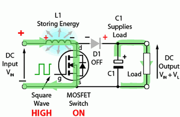
Fig. 2: The two circuit configurations of a buck converter: On-state, when the switch is closed, and Off-state, when the switch is open (Arrows indicate current according to the conventional current model).

Fig. 3: Naming conventions of the components, voltages and current of the buck converter.

Fig. 4: Evolution of the voltages and currents with time in an ideal buck converter operating in continuous mode.

Concept
The conceptual model of the buck converter is best understood in terms of the relation between current and voltage of the inductor. Beginning with the switch open (in the “off” position), the current in the circuit is 0. When the switch is first closed, the current will begin to increase, and the inductor will produce an opposing voltage across its terminals in response to the changing current. This voltage drop counteracts the voltage of the source and therefore reduces the net voltage across the load.
Over time, the rate of change of current decreases, and the voltage across the inductor also then decreases, increasing the voltage at the load. During this time, the inductor is storing energy in the form of a magnetic field. If the switch is opened while the current is still changing, then there will always be a voltage drop across the inductor, so the net voltage at the load will always be less than the input voltage source.
When the switch is opened again, the voltage source will be removed from the circuit, and the current will decrease. The changing current will produce a change in voltage across the inductor, now aiding the source voltage. The stored energy in the inductor’s magnetic field supports current flow through the load. During this time, the inductor is discharging its stored energy into the rest of the circuit. If the switch is closed again before the inductor fully discharges, the voltage at the load will always be greater than zero.
Efficiency factors
Conduction losses that depend on load:
- Resistance when the transistor or MOSFET switch is conducting.
- Diode forward voltage drop (usually 0.7 V or 0.4 V for schottky diode)
- Inductor winding resistance
- Capacitor equivalent series resistance
Switching losses:
- Voltage-Ampere overlap loss
- Frequencyswitch*CV2 loss
- Reverse latence loss
- Losses due driving MOSFET gate and controller consumption.
- Transistor leakage current losses, and controller standby consumption.


