Inter-Integrated Circuits – I2C Basics
In this post, we will discuss all the theoretical concepts that you need to know regarding I2C before programming/testing it on real devices.
Inter-Integrated Circuit (I2C)
As the name suggests, Inter-IC (or the Inter-Integrated Circuit), often shortened as I2C(pronounced eye-two-see), I2C (pronounced eye-squared-see), or IIC, was developed as a communication protocol to interact between different ICs on a motherboard, a simple internal bus system. It is a revolutionary technology developed by Philips Semiconductor (now NXP Semiconductors) in 1982, and is used to connect low speed peripherals (like keyboard, mouse, memory, IO/serial/parallel ports, etc.) to the motherboard (containing the CPU) operating at much higher speed.
These days you can find a lot of devices which are I2C compatible manufactured by a variety of companies (like Intel, TI, Freescale, STMicroelectronics, etc). Somewhere around the mid-1990s, Intel devised the SMBus protocol, a subset of I2C with strict protocols. Most modern day I2C devices support both, I2C and SMBus with little reconfiguration.
I2C Bus Interface
The most compelling thing about the I2C interface is that the devices are hooked up to the I2C bus with just two pins (and hence it is sometimes referred to as Two Wire Interface, or the TWI). Well of course, we do need two more pins for Vcc and ground, but that goes without saying.

As you can see in the above diagram (taken from eeweb.com), all the devices are hooked up to the same I2C bus with just two pins. These devices could be the CPU, or IO devices, or ADC, or any other device which supports the I2C protocol. All the devices connected to the bus are classified as either being Master or Slave (just like SPI). We will discuss about it in a little while.
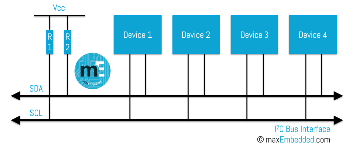
For now, let’s get to know more about the bus itself. The I2C bus consists of two bidirectional “open-drain” lines – SDA and SCL – pulled up with resistors as shown below.
Serial Data Line (SDA)
The Serial Data Line (SDA) is the data line (of course!). All the data transfer among the devices takes place through this line.
Serial Clock Line (SCL)
The Serial Clock Line (SCL) is the serial clock (obviously!). I2C is a synchronous protocol, and hence, SCL is used to synchronize all the devices and the data transfer together. We’ll learn how it works a little later in this post.
Open-Drain Lines
A little while ago (just above the previous image), I mentioned that SDA and SCL are open-drain (also called open-collector) lines pulled up with resistors. What does that mean? It means that the devices connected to the I2C bus are capable of pulling any of these two lines low, but they cannot drive them high. If any of the devices would ever want to drive the lines high, they would simply need to let go of that line, and it would be driven high by the pull up resistors (R1 and R2 in the previous image, or Rp in the next image).
For those who are interested, let’s have a closer look. Others, please skip this section and go to the next to next section (voltage levels and resistor values).
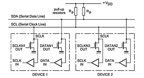
In the above image, you can clearly see the NMOS transistors inside the devices. In order for the device to pull any of the two lines low, it needs to provide a high voltage to the gate of the transistor (that’s how an NMOS transistor operates, right?). If the gate voltage is low, the NMOS transistor is not activated and the corresponding line is driven high.
I2C Data Validity
For the data to be valid on the SDA line, it must not change while the SCL is high. The data on the SDA line should change only and only when the SCL line goes low. If this standard is not followed, the data transfer becomes flawed, in which case it becomes a start/stop sequence (discussed later in this post). The following image illustrates the same.

Voltage Levels and Resistor Values
I2C supports a wide range of voltage levels, hence you can provide +5 volts, or +3.3 volts as Vcc easily, and other lower/higher voltages as well. This gives us a wide range of choices for the values of the pull-up resistors (R1 and R2). Anything within the range of 1k to 47k should be fine, however values lower than 10k are usually preferred.
Master and Slave
The concept of Master and Slave in I2C is quite similar to that of SPI. Just like SPI, all the devices are either Master or Slave. Master is the device which initiates the transfer and drives the clock line SCL. On a single I2C bus, there are usually multiple Slavesconnected to a single Master.
However, just like SPI, we can also have multiple Masters connected to the same I2C bus. Since we want our lives to be a little simpler, we usually avoid such cases, but however I2C supports multi-bus master collision detection and arbitration for such cases (doesn’t make sense? Let’s forget about it for now!).
Speed
I2C supports serial 8-bit bi-directional data transfers up to a speed of 100 kbps, which is the standard clock speed of SCL. However, I2C can also operate at higher speeds – Fast Mode (400 kbps) and High Speed Mode (3.4 Mbps). Most of the devices are built to operate up to speeds of 100 kbps (remember that we discussed that I2C is used to connect low-speed devices?).
I2C Bus Transaction
Alright, now that we are familiar with the I2C bus interface, let’s look into how the data transfer actually takes place through that interface. I2C supports unidirectional as well as bidirectional data transfer as mentioned below. We will discuss about them in detail towards the end of the post.
- Unidirectional Data Transfer
- Master-transmitter to Slave-receiver (Case 1)
- Slave-transmitter to Master-receiver (Case 2)
- Bidirectional Data Transfer
- Master to Slave and Slave to Master (Case 3)
Start/Stop Sequence
In order for the Master to start talking to the Slave(s), it must notify the Slave(s) about it. This is done using a special start sequence. Remember a little while ago we discussed about I2C data validity – that the SDA should not change while the SCL is high? Well, it doesn’t hold good for the start/stop sequence, which is why it makes them special sequences!
When the SCL is high and SDA goes from high to low (as shown in the following diagram), it marks the beginning of the transaction of Master with the Slave(s).

And when the SDA goes from low to high while the SCL is still high (as shown in the following diagram), it marks the end of the transaction of that Masterwith the Slave(s).

NOTE: In between the start and stop sequences, the bus is busy and no other Master(s)(if any) should try to initiate a transfer.
Acknowledge Scheme
As mentioned earlier, I2C transfers 8 bits (1 byte) of data at a time. After the transfer of each byte is complete, the receiver must acknowledge it. To acknowledge, the receiver sends an ACK bit back to the transmitter. Here’s how it goes–
- The transmitter (could be either Master or Slave) transmits 1 byte of data (MSB first) to the receiver during 8 clock pulses of SCL, after which it releases the SDA line i.e. the SDA line becomes HIGH for the ACK clock pulse.
- The receiver (could be either Master or Slave, it depends) is obliged to generate an acknowledge after each byte sent by the transmitter by pulling the SDA line LOW for the ACK clock pulse (9th clock pulse) of SCL.
- So overall, there are 9 SCL clock pulses required to transmit a byte of data. This is shown in the diagram below with the assumption that Masteris the transmitter.

So far so good. But what if the receiver does not (or could not) acknowledge the data sent to it? What happens then? Does the entire system break down?
Well, there are two cases to that situation.
Case 1: Slave is at the receiver’s end
Even in this case, there are two possible cases–
- CASE 1A: The Slave-receiver does not acknowledge the Slave address (hey wait, what’s an address? We’ll get to it shortly). In that case, it simply leaves the SDA line HIGH. Now the Master-transmitter either generates a Stop sequence or attempts a repeated Start sequence.
- CASE 1B: The Slave-receiver acknowledges the Slave address, but after some time it is unable to receive any data and leaves the SDA line HIGH during the ACK pulse. Even in this case, the Master-transmitter does the same – either generate a Stop sequence, or attempt a repeated Start sequence.
Case 2: Master is at the receiver’s end
Now this is a tricky situation. In this case, the Master is the one generating ACK, as well as responsible for generating Start/Stop sequence. Now how does that work out, especially when the transaction ends?
In this case, in order to signal the Slave-transmitter the end of data, the Master-receiverdoes NOT generate any ACK on the last byte clocked out of the Slave-transmitter. In this case, the Slave-transmitter must let go of the SDA line to allow Master to generate a Stop or a repeated Start sequence.
Makes sense? If it is confusing, hopefully it will make more sense when we actually program it for real.
I2C Device Addressing
Somewhere in the beginning of the tutorial, I mentioned that we can hook up a lot of devices to the I2C bus. But the Master can talk with only one of the Slaves at a time. Now how does that happen?
This is pretty similar to the situation inside a classroom. There is one teacher (Master) and a ridiculous number of students (Slaves). The teacher wants to ask a question to one of the students. How does she do that? Well, we do have a name, right? All the students have a unique name (address), and the teacher calls out the name first, right? Hey Max, could you explain why do we need casex statements in Verilog? Sounds familiar? Good old school days, eh?
Well, this is exactly what happens in case of I2C bus transaction. Every device hooked up to the bus has a unique address. As per the I2C specifications, this address is either 7 bits long, or 10 bits long. 10-bit addresses are rare, and since I am lazy, I am gonna skip it for now.
When we have 7-bit address, we can have up to a maximum of 27 = 128 devices hooked up to the I2C bus, with addresses 0 to 127. Now when the Master calls out to the Slave(s), it still needs to send out 8 bits of data. In this case, the Master appends an extra Read/Write (R/W’) bit to the 7 bits of address (note that W’ means Write complemented). Thus, the R/W’ bit is added to the LSB of the data byte. So now, the data sent looks somethings like this–

Why should I bother about it?
Well, this is a question which I expect all the newbies to ask. Unfortunately most of them don’t and then end up being frustrated. Why the heck is my I2C not working?!
Let’s take a scenario. You have an external EEPROM which you want to interface using I2C with your processor. You know that the address of the EEPROM is 0x50. You send this address to the bus expecting the EEPROM device to acknowledge. Does it acknowledge? Heck, NO!
So what’s the problem here? Yes, you guessed it right (hopefully). You forgot about the R/W’ bit! The address 0x50 is actually the 7-bit address (0b1010000).
Let’s make it right. Say you wanna perform page write operation on the EEPROM device. This means that you wish to write to the device and hence the R/W’ bit must be set to 0. Why you ask? Because the write is complemented. For read, R/W' = 1, whereas for write, R/W' = 0. Makes sense?
So what should be the correct (modified) address?
0x50 << 1 + 0x0 = 0xA00b1010000 << 1 + 0b0 = 0b10100000(Note: << refers to left shift operation) |
If you wanna perform sequential read operation on the same EEPROM device, what would be your (modified) address?
0x50 << 1 + 0x1 = 0xA10b1010000 << 1 + 0b1 = 0b10100001(Note: << refers to left shift operation) |
So, we can generalize that for write operations, the 8 bit address is even, whereas for read operations, the 8 bit address is odd.
I2C Data Transfer Protocol
Now that we are familiar with the I2C bus transactions and device addressing, let’s see how to transfer data using the I2C protocol and have a 10,000 foot view of the entire bus transaction.
Timing Diagram
Let’s look at the timing diagram of an entire transaction – from start to stop!

Let’s analyze it first. Before we begin, we all know what these slanted lines mean, right? The slanted lines are a representation of slew rate of the device/bus/system. Ideally, whenever a signal changes its state (from high to low or vice-versa), it is supposed to do so immediately. But in real scenario, it is almost impossible for it to happen without a time lag. The slanted lines refer to these time lags, also known as slew.
Alright, back to where we were.
- The transaction starts with a START sequence.
- After the START sequence, the Master has to send the address of the Slave it wants to talk to. That’s the 7-bit ADDRESS (MSB first) followed by R/W’ bit determining whether you want to read from the device or write into it.
- The Slave responds by acknowledging the address. Yay! If it doesn’t send the ACK, we know what the Master does, right?
- Once the Slave acknowledges the address, it means that it is now ready to send/receive data to/from the Master. Thus begins the data transfer. The DATA is always of 8 bits (MSB first), and the receiver has to send the ACK signal after each byte of data received.
- When the transaction is over, the Master ends it by generating a STOP sequence. Alternatively, Master could also begin with a repeated START.
There are three possible cases of data transfer–
- Case 1: Master-transmitter to Slave-receiver
- Case 2: Slave-transmitter to Master-receiver
- Case 3: Bi-directional (R/W) in same data transfer
Case 1: Master (Transmitter) to Slave (Receiver) Data Transfer
Let’s have a look at the entire transaction first and then analyze it.

- The Master sends the START sequence to begin the transaction.
- It is followed by Master sending 7-bit Slave address and the R/W’ bit set to zero. We set it to zero because the Master is writing to the Slave.
- The Slave acknowledges by pulling the ACK bit low.
- Once the Slave acknowledges the address, Master can now send data to the Slave byte-by-byte. The Slave has to send the ACK bit after every byte it receives.
- This goes on till Slave can no longer receive data and does NOT send the ACK bit.
- This is when the Master realizes that the Slave has gone crazy (not accepting anymore) and then STOPs the transaction (or reSTART).
We see that the data transfer never changes its direction. Data always flows from Master to Slave, which makes the setup quite easy.
An example of this case would be like performing page write operations on a EEPROM chip.
Case 2: Slave (Transmitter) to Master (Receiver) Data Transfer
Let’s look at the entire transaction again.

- The Master sends the START sequence, followed by the 7-bit Slaveaddress and the R/W’ bit set to 1.
- We set R/W’ bit to 1 because the Master is reading from the Slave.
- The Slave acknowledges the address, thus ready to send data now.
- Slave keeps on sending data to the Master, and the Master keeps on sending ACK to the Slave after each byte until it can no longer accept any more data.
- When the Master feels like ending the transaction, it does not send the ACK, thus ending with the STOP sequence.
An example of this case could be an Analog to Digital Converter (ADC) sending data to the microcontroller continuously. The microcontroller accepts data as long as it wants to, after which it stops/finishes execution.
Case 3: Bi-directional Read and Write in same Data Transfer
Once again, let’s look at the entire transaction first!

- The Master sends out the START sequence, followed by the 7-bit Slaveaddress and the R/W’ bit.
- The Slave acknowledges the address.
- Depending upon the value of the R/W’ bit, read/write operations are performed (like the above two cases).
- Whatever the case it may be, it always ends with the receiver not sending the ACK.
- Until now, in the previous two cases, we have seen that the Master would close the connection. But in this case, the Master attempts a repeated START.
- And the entire process repeats again, until the Master decides to STOP.
As we can see, a change of direction of data transfer might happen depending upon the R/W’ bits in the entire transaction.
An example of this case could be performing sequential read from a EEPROM chip. It is bi-directional because the CPU first writes the address from where it would like to start reading, followed by reading from the device. It is like, unless you tell the device from where you would like to start reading, how would it start sending you the data?
Clock Stretching
So far so good. Now let’s look at a very plausible complication. Suppose Master is reading data from the Slave. Everything goes on good as long as the Slave returns the data. What if… what if the Slave is not just ready yet? This is not an issue with devices like ADC or EEPROM, but with devices like a microcontroller. What if the Slave is a microcontroller, and the Master requests for a data which is not there in its cache. This would require the microcontroller to perform context switching, force it to search for it in the RAM, store it back in cache and then send it to the Master. This could (and definitiely would) take a much longer time than the clock pulses of the SCL, and everything would just go wrong!
Fortunately, there is a way, called Clock Stretching. The Slave is allowed to hold the clock line low until it is ready to give out the result. The Mastermust wait for the clock to go back to high before continuing with its work.
This is the only instance in the entire I2C protocol where the Slave is drives the clock line SCL. In many processors and microcontrollers, the low level hardware does this for us, so that we don’t have to worry about it while writing the code.
Why I2C?
Now that we are almost done with the basics of I2C communications, let’s take a moment to jot down some advantages of I2C.
- I2C requires least number of pins (just two pins) to perform serial data transfer.
- The receiver always sends feedback to the transmitter (ACK) conveying a successful transmission, which leads to higher noise immunity as well.
- Even though it has a slow standard speed of 100 kHz, modern I2C specifications support up to 3.4 MHz clock speed.
Summary
- I2C is an 8-bit bidirectional synchronous serial communication protocol requiring only two wires for operation.
- The I2C bus consists of two open-drain lines – SDA (data) and SCL (clock).
- Several devices, being either Master or Slave, can be connected to the bus. The Master device must initiate the transfer and drive the clock line (SCL).
- I2C supports the standard speed of 100 kbps, up to a maximum speed of 3.4 Mbps.
- Master must generate unique Start and Stop conditions in order to mark the beginning and end of a transaction.
- The receiver must send the ACK bit after every byte that it receives, failing which the Master may either Stop the transaction or attempt a repeated Start.
- Every device connected to the I2C bus has either 7-bit or 10-bit address. An additional R/W’ bit is added to the address by the Master to determine whether it wants to read or write from/to the device.
- Data transfer can be unidirectional (Master to Slave OR vice-versa) or bidirectional.
- Slave can hold the clock line low until it is ready with the result to be sent to the Master, called Clock Stretching.

